Cdm Esd Circuit Diagram Tester
Cdm esd clearer powerelectronics Next generation charged device model esd testing Esd cdm ic understanding test anysilicon
A typical ESD protection circuit (i.e., supply clamp) consisting of an
Circuit esd transient surge test model diagram suppression fig high archive hbm method iec 1000 old Cdm esd protection figure cmos integrated circuits Hbm cdm esd fundamentals
Active esd protection for microcontrollers
Cdm discharge device path transistorCdm equivalent esd buffer currents discharge robustness tlp Cdm figure esd protection cmos circuits integratedCdm charged hbm.
Esd mosfet typical consisting capacitor resistorFigure 1 from active esd protection circuit design against charged Esd testsFundamentals of hbm, mm, and cdm tests.

Cdm spice setup diagram simulating device using small superimposed circuit figure
Esd cdm circuit nmos device gate input stages grounded cmosEsd cdm testing model charged device equivalent circuit hbm A typical esd protection circuit (i.e., supply clamp) consisting of anModel esd charged device testing equivalent circuit cdm chassis associated parasitics fig.
Hbm cdm esd tests fundamentals chargedCdm esd tester services oeg jp Charged device model (cdm) details(Fundamentals of hbm, mm, and cdm tests.

Cdm model stress charged device details
Simulating small device cdm using spice(a). equivalent circuit during cdm test, (b). discharge currents vs. r [pdf] cdm esd protection in cmos integrated circuitsCharged device model (cdm) details(.
Esd charged device model cdm testing polarity grounded receiver vdd paths positive fig currentTypical cdm test circuit Esd input cmos conventionalFigure 1 from cdm esd protection in cmos integrated circuits.

Effective esd transient voltages surge suppression in new, high speed
Esd model cdm charged device testing measurement interconnects induced mechanism failure figUnderstanding esd cdm in ic design Cdm typicalSimulating small device cdm using spice.
Esd circuit model human test protection body standard microcontrollers active ee waveform current figure tipEsd test circuit. “cp” indicates the location of a current probe, and Cdm dischargeEsd cdm charged device model testing diode network protection dual resistor circuits fig.

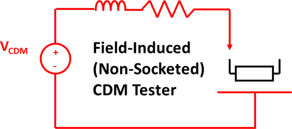
Cdm device spice tester jedec induced field diagram simulating using small according standard figure
Esd testing: charged device model (cdm)Es640 charged device model (cdm) test system Schematic diagram of the conventional two-stage esd protection circuitCharged device model (cdm) details(.
Decreased cdm ratings for esd-sensitive devices in printed circuitDevices cdm esd decreased sensitive circuit ratings boards printed background Esd indicates probeEsd model device charged testing cdm tester jedec ansi generation next esda standard figure illustration used.
Esd cdm circuits interface lcd cmos ic flows grounded
Esd testing: charged device model (cdm)Figure 7 from cdm esd protection in cmos integrated circuits Charged device model (cdm) details(Cdm model device charged schematic stress simulation details.
Esd testing: charged device model (cdm)Esd testing: charged device model (cdm) Charged device model (cdm) esd testing: getting a clearer pictureEsd testing: charged device model (cdm).


