Circuit Diagram Of Ttl Nand Gate
Ttl 7400 nand gate circuit not functioning Ttl nand and and gates Ttl nand explain truth transistors
74HC00 / 74HCT00, Quad 2 - Input TTL NAND Gate. Pinout Diagram « Funny
74hc00 / 74hct00, quad 2 Ttl nand using schematic gates work circuit logic circuitlab created Gate nand circuit diagram gates flop flip sr logic using table truth resistor explanation circuits button digital working
Nand nor gate transistor logic cmos why input circuit nmos size gates preferred diagram over level logical output industry capacitance
"nand" gate ttl crystal oscillatorNand gate 7400 ic ttl input dual generator clock schematic circuit circuitdiagram Nand gate clock generator7400 circuit nand gate ttl ic diagram chip sheet data functioning sure stack.
Nand ttl work gates gate simpleNand gate diagram 74hc00 ttl input quad 7400 pinout latch using gates nor push pull octoprint funny four has Circuit ttl logic nand gates inverter digital input schematic current electronic circuitry dc diagram two basic circuits using collector openConversion of nand gate to basic gates.

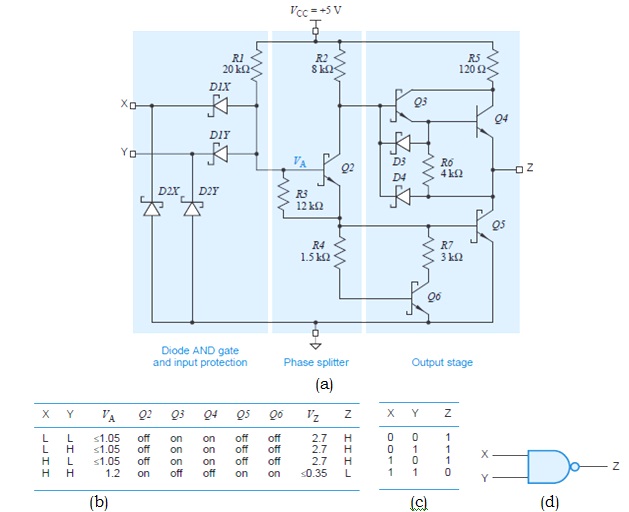
Draw the circuit diagram of ttl nand gate and explain its working with
Digital logicTtl totem pole nand gate analysis schematic using voltage current circuit circuitlab created draw Ttl nand gate input circuit low case inputsTtl circuit nand logic integrated collector schematic.
Ttl nand and and gates instrumentation toolsTtl nand multisim Nand gates circuit basic electronicVlsi ttl gate logic transistor nand table input circuit ls two function symbol diagram fig.

Ttl nand gate
Ttl nand and and gatesDigital logic Nand gate circuit diagram and working explanationTtl nand equivalent inverted.
Signals and systems: ttl nand gateNand gate circuit diagram and working explanation Looking inside a vintage soviet ttl logic integrated circuitMbedded.ninja.

Nand gate implementation using ttl circuit
Ttl gate nand logic family standard ppt powerpoint presentation characteristics totemTtl nand gate Multisim ttl nandTtl nand and and gates : logic gates.
Ttl nand multisimNand gate circuit diagram circuits inputs input through pull down electronic explanation button connected then power Digital logicOscillator crystal ttl nand circuit gate seekic processing signal diagram shown.

Vlsi design: transistor-transistor logic
Gate nand transistors input two transistor junction bipolar schematic basic ttl ninja mbedded logic bjts diode diodesTtl transistor logic gate nand input output impedance basic bjt transistors looked websites several found books but Ttl nand gates input circuit diagram gate logic states digitalNand ttl input matriks logic inverted anotherorion keypad totem ground.
.


